The Next Wave of Machine Vision Interfaces
This new wave of interface design choices is significantly influenced by the electronics, mobile, and personal computing markets.
By Ed Goffin
One of the biggest game changers for machine vision has been the introduction and standardization of interfaces. In the earlier years of this century GigE Vision and Camera Link, followed by CoaXPress (CXP) and USB3 Vision, all made it easier to design, deploy, and integrate machine vision cameras, sensors, and processing.
As a result, machine vision moved from research labs to manufacturing floors in an impactful way, and spread to new markets including security and defense, transportation and logistics, and medical diagnostics.
Jump ahead a few decades, and we’re seeing new interface technologies and standards that will further propel machine vision market growth. Driving this is increasing demand for higher bandwidth image transfer and processing capabilities as automated processes beyond faster and more sophisticated, combined with advancements that make edge and embedded technologies attractive for vision systems.
The first wave of standardized machine vision interfacesborrowed heavily from adjacent industries, including broadcast and telecommunications. Similarly, this new wave of interface design choices is significantly influenced by the electronics, mobile, and personal computing markets.
PCIe and Thunderbolt Eases CPU Requirements
Peripheral Component Interconnect Express (PCIe) is commonly used to connect hardware devices to a computer’s motherboard, with several machine vision component manufacturers supplying PCIe frame grabbers supporting common interface standards. The frame grabber plugs into an available card slot on the PC and communicates over PCIe.
It has proven to be a straightforward approach to connectivity for the past decade, until card slots started disappearing on PCs. Small form factor edge, single-board, and embedded computing devices further exacerbate the connectivity challenge.
In comparison, advances in the Thunderbolt standard universalized the connectivity technology beyond Mac devices while providing bidirectional data rate advantages and multiprotocol PCIe, DisplayPort, and USB support. Early concepts for Thunderbolt-enabled machine vision cameras never gained market traction, and instead the industry moved to the USB3 Vision standard. As the Thunderbolt standard has evolved, there’s a much clearer opportunity for the technology in machine vision.
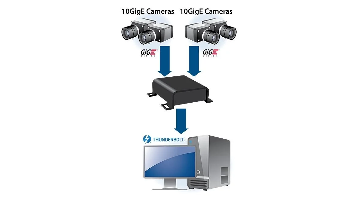
One approach combines the advantages of GigE Vision, PCIe, and Thunderbolt. In this solution, an external frame grabber converts GigE Vision cameras into PCIe cameras and transmits high bandwidth (up to 22.5 Gbps) imaging and video data with low, predictable latency over a standard cable directly to a Thunderbolt/USB 4 port or Thunderbolt 3/4 USB-C port. By eliminating the need for a desktop computer with an available PCIe card slot for a traditional frame grabber, designers can reduce system size, cost, and power by using smaller form factors laptops, embedded computers, and single-board computers.
GigE Vision to Thunderbolt frame grabbers help eliminate CPU bottlenecks for higher-bandwidth imaging applications. Image Source: Pleora Technologies
This approach marries the cabling, multicasting, and device availability benefits of GigE Vision, the efficiency of a PCIe frame grabber, and the “plug-and-play” convenience of Thunderbolt. In addition, by extending the PCIe bus to the external frame grabber, designers can optimize CPU usage with a built-in direct memory access (DMA) engine that acquires and copies full machine vision image data to the memory of the host PC. With active optical cables reaching distances up to 50 meters, system designers can anticipate cabling prices to drop as Thunderbolt ports become standard on a wider range of devices.
The combination of PCIe with Thunderbolt provides an optimized peripheral solution to upgrade the performance of 10G and beyond vision systems, particularly thanks to its ability to free valuable processing resources for application tasks. For imaging device designers, PCIe to Thunderbolt embedded interfaces and IP cores will provide a straightforward approach to developing higher bandwidth solutions.
GigE Vision and RoCEv2
While Thunderbolt promises to bring a new alternative to imaging device and system design, the GigE Vision standard is not sitting idly on the sidelines. GigE Vision 3.0, currently in development with the Association for Advancing Automation (A3) and its GigE Vision Technical Committee, is also addressing CPU utilization by leveraging Remote Direct Memory Access (RDMA) over Converged Ethernet (RoCE) technology. The updated, backwards compatible standard is expected to be released in 2025.
RoCE was initially developed in 2010 to bring the RDMA benefits of high throughput and low CPU utilization to standard Ethernet networks. It is now the industry standard for data transfer in high-performance computing, enterprise networks, data centers, and cloud computing. RoCE v1 runs over Layer 2 Ethernet, meaning it is limited to a single Ethernet broadcast domain. RoCEv2, however, operates over Layer 3, allowing it to be routable across IP networks and making it suitable for larger and more complex network topologies.
For machine vision, RoCEv2 allows imaging data to be transferred directly from a camera or sensor to the memory of the host processor without involving the CPU, operating system (OS), or cache. Adapting the open standard technology of RoCEv2 to coexist within the GigE Vision standard provides a clear path towards Ethernet-based imaging solutions supporting bandwidths of 50…100…200…400 Gbps without impacting receive-side latency.
“Zero copy” image transfer provides critical performance and power benefits to machine vision systems. Bypassing the CPU lowers glass-to-glass latency, ensuring real-time data processing and analysis critical for applications requiring immediate response such as automated inspection and robotic guidance. Freeing CPU resources from image transfer requirements provides more horsepower for value-added imaging processing applications, while also reducing overall power consumption.
Several vendors are anticipating the release of the GigE Vision 3.0 standard with RoCEv2-enabled embedded interfaces, IP cores, and hardware reference designs. Integrating higher bandwidth and lower CPU usage into the GigE Vision standard, and ensuring interoperability between vendor solutions, will solidify Ethernet as the de facto connectivity solution for machine vision applications while helping drive solutions into new markets.
Embedded Design Options
It’s impossible to ignore the impact that embedded and edge computing is having on machine vision system and device design. At a recent manufacturing trade show, I was struck by how commonplace small footprint sensor-based imaging solutions are in automated inspection, logistics and handling, and robotics systems. There is a definite trend towards embedded imaging solutions, in particular devices that incorporate AI-based analysis or local edge processing decision-making.
There are many parallels to the earlier days of vision, or even today with Thunderbolt and RoCEv2, where proven technologies are migrating into machine imaging and system design. Two prime examples are Scalable Low-Voltage Signaling with Embedded Clock (SLVS-EC) and the Mobile Industry Processor Interface (MIPI) protocols.
SLVS-EC is a high-speed interface developed by Sony for high-resolution image sensors, supported by a simple protocol that makes it easy to create cameras. Featuring an embedded clock signal that improves the reliability of data transmission, it is ideal for applications requiring higher speed, transmission over longer distance, and low power consumption. The scalability of the SLVS-EC interface means it can support different levels of performance; from lower power, single-lane configurations to high-speed, multi-lane designs.
SLVS-EC is specifically designed to be compatible with high-end image sensors, including those used in advanced machine vision systems. This compatibility ensures that SLVS-EC can handle the large data outputs of modern image sensors, supporting high-quality image capture and processing.
Solutions integrating SLVS-EC are deployed in advanced driver assistance systems (ADAS), broadcast equipment, medical imaging solutions such as endoscope and ultrasound, and surveillance systems. For industrial automation and inspection systems, SLVS-EC is well-suited to quality control, defect detection, and production line monitoring where high-speed image capture and processing are crucial.
MIPI is a set of protocols developed by the MIPI Alliance for the integration of high-speed interfaces in mobile and mobile-influenced devices. MIPI protocols are widely used across various industries due to their efficiency, scalability, and low power consumption. It is a protocol probably most associated with mobile phones, where the MIPI Camera Serial Interface (CSI-2) and DSI (Display Serial Interface) connect camera modules to processors and displays.
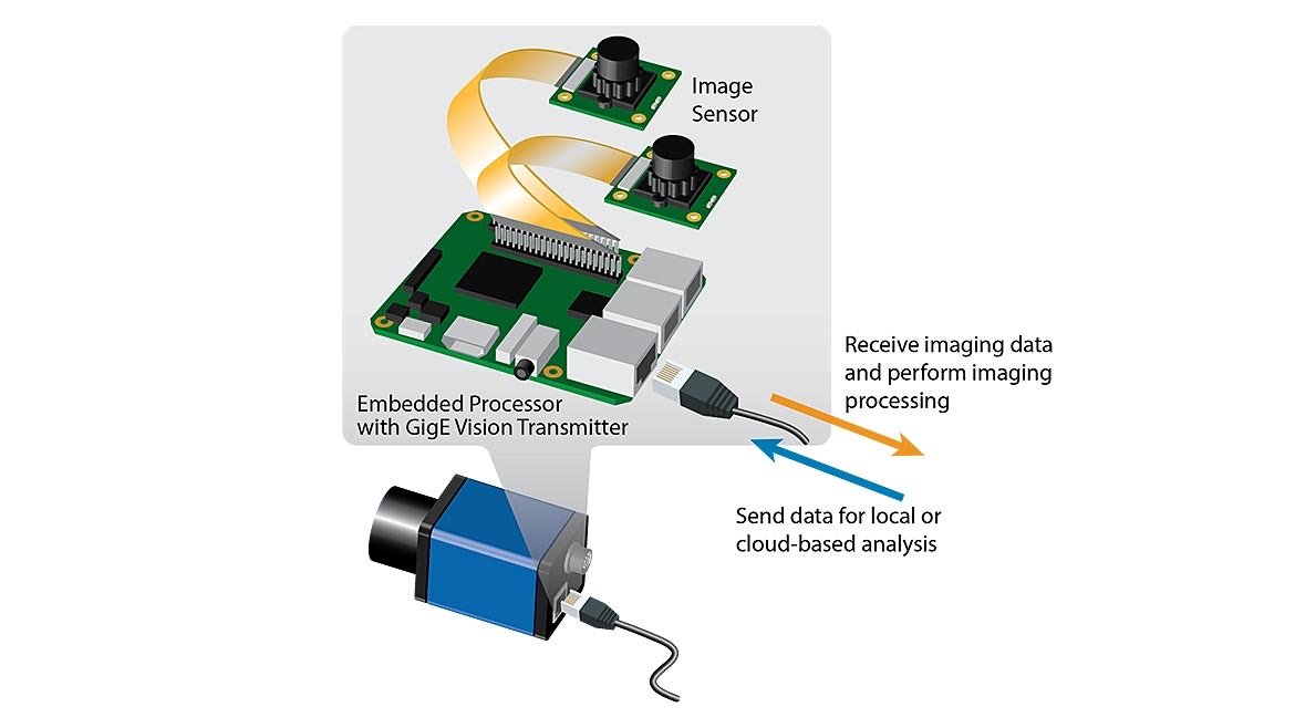
For embedded designers MIPI offers a low-cost alternative to traditional machine vision solutions, though the cost of software development to ensure device and system level interoperability needs to be considered and is often overlooked. One approach to this challenge is vision standard compliant software transmitters, which convert embedded devices into GigE Vision, GenICam devices. This enables seamless standards-based integration and device control between embedded solutions and machine vision and edge processing.
Software transmitter solutions convert embedded devices to fully compliant GigE Vision, GenICam devices that integrate with off-the-shelf machine vision processing. Image Source: Pleora Technologies
Hardware manufacturers including NVIDIA and Raspberry Pi provide MIPI interfaces, making it easy to connect to image sensors and develop a complete camera system. MIPI protocols are highly scalable, allowing for the use of multiple lanes to increase data throughput as needed. This scalability supports a wide range of applications, from simple low-power sensors to high-performance cameras and displays, making MIPI malleable to different system requirements.
The Interface Evolution
The vision industry is on the cusp of its next interface evolution. Time-honored standards such as GigE Vision and PCIe are advancing in response to increasing performance demands, while the rise of embedded and edge processing is presenting new interface options. For both system and device designers, this evolution is integral to meeting the next set of performance, cost, and interoperability demands.


